(Hong Kong)

Product Summary
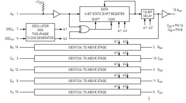
The mc14495p1 is a Hex Contact Bounce Eliminator. The mc14495p1 is constructed with complementary MOS enhancement mode devices, and is used for the elimination of extraneous level changes that result when interfacing with mechanical contacts. The mc14495p1 takes an input signal from a bouncing contact and generates a clean digital signal four clock periods after the input has stabilized. The mc14495p1 will remove bounce on both the “make” and the “break” of a contact closure. The clock for operation of the mc14495p1 is derived from an internal R–C oscillator which requires only an external capacitor to adjust for the desired operating frequency (bounce delay). The clock may also be driven from an external clock source or the oscillator of another mc14495p1.
Parametrics
mc14495p1 absolute maximum ratings: (1)VDD, DC Supply Voltage Range: –0.5 to +18.0 V; (2)Vin, Vout, Input or Output Voltage Range: –0.5 to VDD + 0.5 V; (3)Iin, Input Current: ±10 mA; (4)PD, Power Dissipation, per Package: 500 mW; (5)TA, Ambient Temperature Range: –55 to +125 ℃; (6)Tstg, Storage Temperature Range: –65 to +150 ℃; (7)TL, Lead Temperature: 260 ℃.
Features
mc14495p1 features: (1)Diode Protection on All Inputs; (2)Six Debouncers Per Package; (3)Internal Pullups on All Data Inputs; (4)Can Be Used as a Digital Integrator, System Synchronizer, or Delay Line; (5)Internal Oscillator (R–C), or External Clock Source; (6)TTL Compatible Data Inputs/Outputs; (7)Single Line Input, Debounces Both “Make” and “Break” Contacts; (8)Does Not Require “Form C” (Single Pole Double Throw) Input Signal; (9)Cascadable for Longer Time Delays; (10)Schmitt Trigger on Clock Input (Pin 7); (11)Supply Voltage Range = 3.0 V to 18 V; (12)Chip Complexity: 546 FETs or 136.5 Equivalent Gates.
Diagrams