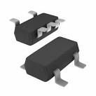
Product Summary
The 74LVC273PW is a low-voltage Si-gate CMOS device, superior to most advanced CMOS compatible TTL families. The 74LVC273PW has eight edge-triggered , D-type flip-flops with individual D inputs and Q outputs. The common clock (CP) and master reset (MR) inputs load and reset (clear) all flip-flops simultaneously. The state of each D input, one set-up time before the LOW-to-HIGH clock transition, is transferred to the corresponding output (Qn) of the flip-flop. The 74LVC273PW is useful for applications where the true output only is required and the clock and master reset are common to all storage elements.
Parametrics
74LVC273PW absolute maximum ratings: (1)VCC DC supply voltage: -0.5 to +6.5 V; (2)IIK DC input diode current: -50 mA; (3)VI DC input voltage: -0.5 to +5.5 V; (4)IOK DC output diode current: ±50 mA; (5)VO DC output voltage: -0.5 to VCC +0.5 V; (6)IO DC output source or sink current: ±50 mA; (7)IGND, ICC DC VCC or GND current: ±100 mA; (8)Tstg Storage temperature range: -65 to +150 ℃; (9)PTOT Power dissipation per package-plastic mini-pack (SO): 500 mW; -plastic shrink mini-pack (SSOP and TSSOP): 500 mW.
Features
74LVC273PW features: (1)Wide supply voltage range of 1.2V to 3.6V; (2)Conforms to JEDEC standard 8-1A; (3)Inputs accept voltages up to 5.5V; (4)CMOS low power consumption; (5)Direct interface with TTL levels; (6)Output drive capability 50Ω transmission lines @ 85℃.
Diagrams
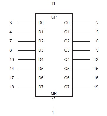
| Image | Part No | Mfg | Description |  |
Pricing (USD) |
Quantity | ||||||||||||
|---|---|---|---|---|---|---|---|---|---|---|---|---|---|---|---|---|---|---|
 |
 74LVC273PW |
 NXP Semiconductors |
 Flip Flops OCT D F/F POS EDGE W/RESET |
 Data Sheet |
 Negotiable |
|
||||||||||||
 |
 74LVC273PW,112 |
 NXP Semiconductors |
 Flip Flops OCT D F/F POS EDGE |
 Data Sheet |

|
|
||||||||||||
 |
 74LVC273PW,118 |
 NXP Semiconductors |
 Flip Flops 3.3V OCTAL POS D-TYPE |
 Data Sheet |

|
|
||||||||||||
 (Hong Kong)

