(Hong Kong)

Product Summary
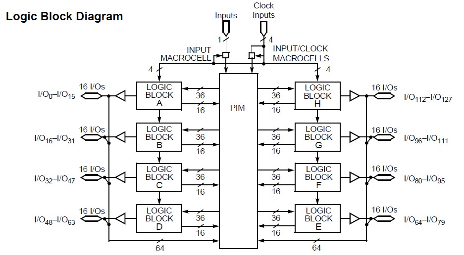
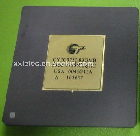
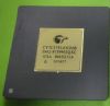
The CY7C375I-83GMB is an in-system reprogrammable complex programmable logic device (CPLD) and is part of the flash370i family of high-density, high-speed CPLDs. Like all members of the flash370i family, the CY7C375I-83GMB is designed to bring the ease of use and high performance of the 22V10 to high-density PLDs. Like all of the UltraLogic FLASH370i devices, the CY7C375I-83GMB is electrically erasable and in-system reprogrammable (ISR), which simplifies both design and manufacturing flows thereby reducing costs. The cypress ISR function is implemented through a JTAG serial interface. Data is shifted in and out through the SDI and SDO pins. The ISR interface is enabled using the programming voltage pin (ISREN). Additionally, because of the superior routability of the flash370i devices, ISR often allows users to change existing logic designs while simultaneously fixing pinout assignments.
Parametrics
CY7C375I-83GMB absolute maximum ratings: (1)Storage temperature: –65°C to +150°C; (2)Ambient temperature with power applied: –55°C to +125°C; (3)Supply voltage to ground potential: –0.5V to +7.0V; (4)DC voltage applied to outputs in high-z state: –0.5V to +7.0V; (5)DC input voltage: –0.5V to +7.0V; (6)DC program voltage: 12.5V; (7)Output current into outputs: 16 mA; (8)Static discharge voltage: > 2001V (per MIL-STD-883, Method 3015); (9)Latch-up current: > 200 mA.
Features
CY7C375I-83GMB features: (1)128 macrocells in eight logic blocks; (2)128 I/O pins; (3)Five dedicated inputs including 4 clock pins; (4)In-System Reprogrammable Flash technology: JTAG Interface; (5)Bus Hold capabilities on all I/Os and dedicated inputs; (6)No hidden delays; (7)High speed: fMAX = 125 MHz; tPD = 10 ns; tS = 5.5 ns; tCO = 6.5 ns; (8)Fully PCI compliant; (9)3.3V or 5.0V I/O operation; (10)Available in 160-pin TQFP, CQFP, and PGA packages.
Diagrams