(Hong Kong)


Product Summary
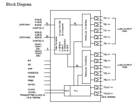
The thc63lvd1023 is a 160MHz 67Bits LVDS Transmitter which is designed to suport Single Link transmission between Host and Flat Panel Display up to 1080p(60Hz) resolutions and Dual Link transmission between Host and Flat Panel Display up to 1080p(120Hz). The thc63lvd1023 converts 67bits of CMOS/TTL data into LVDS (Low Voltage Differential Signaling) data stream. The transmitter can be programmed for rising edge or falling edge clocks through a dedicated pin, and support double edge inputs. In Dual Link, the transmit clock frequency of 160MHz, 67bits of RGB data are transmitted at an effective rate of 1.12Gbps per LVDS channel. In Asynchronous mode, the thc63lvd1023 has 2 independent 35Bits transmitter.
Parametrics
thc63lvd1023 absolute maximum ratings: (1)Supply Voltage (VCC): -0.3V ~ +4.0V; (2)CMOS/TTL Input Voltage: -0.3V ~ (VCC + 0.3V); (3)LVDS Driver Output Voltage: -0.3V ~ (VCC + 0.3V); (4)Output Current: -30mA ~ 30mA; (5)Junction Temperature: +125℃; (6)Storage Temperature Range: -55℃ ~ +125℃; (7)Reflow Peak Temperature / Time: +260℃ / 10sec.; (8)Maximum Power Dissipation @+25℃: 2.4W.
Features
thc63lvd1023 features: (1)Wide dot clock range suited for TV Signal (480i-1080p), PC Signal (VGA-QXGA) TTL/CMOS Input: 10-160MHz LVDS Output: 20-160MHz; (2)PLL requires No external components; (3)Flexible Input/Output mode: Single/Dual TTL IN, Single/Dual LVDS OUT, Double edge input for Single TTL IN/Dual LVDS OUT, Input port SW for Single TTL IN/Dual LVDS OUT, Asynchronous Dual TTL IN/Dual LVDS OUT; (4)Clock edge selectable; (5)3 LVDS data mapping for simplifying PCB layout.; (6)Pseudo Random pattern generation circuit; (7)Supports Reduced swing LVDS for Low EMI; (8)Power down mode; (9)Low power single 3.3V CMOS design; (10)Backward compatible with THC63LVD1023; (11)144pin LQFP.
Diagrams