(Hong Kong)

Product Summary
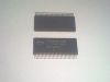
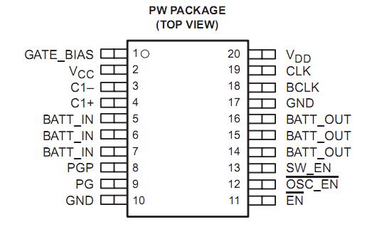
The tps9103pwr is a highly integrated power supply for depletion-mode GaAs power amplifiers (PA) in cellular handsets and other wireless communications equipment. Functional integration and low-profile packaging combine to minimize circuit-board area and component height requirements. The tps9103pwr includes: a p-channel MOSFET configured as a high-side switch to control the application of power to the PA; a driver for the high-side switch with a logic-compatible input; a charge pump to provide negative gate-bias voltage; and logic to prevent turn-on of the high-side switch until gate bias is present. The high-side switch has a typical on-state resistance of 135 mΩ. The tps9103pwr is available in a 20-pin thin shrink small-outline package (TSSOP) or in chip form. Contact factory for die sales. The tps9103pwr operates over a junction temperature range of –25°C to 125°C.
Parametrics
tps9103pwr absolute maximum ratings: (1)High-side switch input voltage range, BATT_IN: –0.3 V to 15 V; (2)Supply voltage range, VCC, VDD: –0.3 V to 7 V; (3)Differential voltage, |BATT_IN|–|GATE_BIAS|: 15 V; (4)Input voltage range, SW_EN, EN, CLK, OSC_EN, PG: –0.3 V to VCC + 0.3 V; (5)GATE_BIAS: –5.5 V; (6)Output current, PG: 5 mA; (7)Output current, BCLK: 50 mA; (8)Output current, GATE_BIAS: 10 mA; (9)Output current, BATT_OUT: 2 A; (10)Peak output current, BATT_OUT: 4 A; (11)Maximum external clock frequency, CLK: 100 kHz; (12)Junction temperature range, TJ: –25°C to 150°C; (13)Storage temperature range, Tstg: –65°C to 150°C.
Features
tps9103pwr features: (1)Charge Pump Provides Negative Gate Bias for Depletion-Mode GaAs Power Amplifiers; (2)Buffered Clock Output to Drive Additional External Charge Pump; (3)135-mΩ High-Side Switch Controls Supply Voltage to the GaAs Power Amplifier; (4)Power-Good Circuitry Prevents High-Side Switch Turn-on Until Negative Gate Bias is Present; (5)Charge Pump Can Be Driven From the internal Oscillator or An External Clock; (6)10-μA Maximum Standby Current; (7)Low-Profile (1.2-mm Max Height), 20-Pin TSSOP Package.
Diagrams
| Image | Part No | Mfg | Description |  |
Pricing (USD) |
Quantity | ||||
|---|---|---|---|---|---|---|---|---|---|---|
 |
 TPS9103PWR |
Texas Instruments (VA) |
IC GAAS POWER SUPPLY 20-TSSOP |
Data Sheet |
Negotiable |
|
||||
| Image | Part No | Mfg | Description | |
Pricing (USD) |
Quantity | ||||
 |
TPS9103 |
Other |
|
Data Sheet |
Negotiable |
|
||||
|
TPS9103PWR |
Texas Instruments (VA) |
IC GAAS POWER SUPPLY 20-TSSOP |
Data Sheet |
Negotiable |
|
||||
|
TPS9104 |
Other |
|
Data Sheet |
Negotiable |
|
||||
 |
TPS9104IPT |
Texas Instruments |
IC CST PWR SUPP/AUDIO SYS 48LQFP |
Data Sheet |
Negotiable |
|
||||
|
TPS9110 |
Other |
|
Data Sheet |
Negotiable |
|
||||
|
TPS9111 |
Other |
|
Data Sheet |
Negotiable |
|
||||