(Hong Kong)

Product Summary
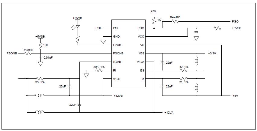
The wt7525y is a PC power supply supervisor. The wt7525y provides protection circuits, power good output (PGO), fault protection latch (FPOB), and a protection detector function (PSONB) control. It can minimize external components of switching power supply systems in personal computer. The Over / Under Voltage Detector (OVD / UVD) monitors V33, V5, V12A, V12B and V12C input voltage level. The Over Current Detector (OCD) monitor IS33, IS5, IS12A, IS12B and IS12C input current sense. When OVD or UVD or OCD detect the fault voltage level, the FPOB is latched HIGH and PGO go low. The latch can be reset by PSONB go HIGH. There is 3.5 ms delay time for PSONB turn off FPOB. When OVD and UVD and OCD detect the right voltage level, the power good output (PGO) will be issue.
Parametrics
wt7525y absolute maximum ratings: (1)Supply voltage, VCC, V12A: –0.3 to 16 V; (2)PGI, PSONB: –0.3 to VCC + 0.3(Max. 7V) V; (3)V5, V33, I5, I33: –0.3 to V12A Input voltage + 0.3(Max. 7V) V; (4)V12B, I12A, I12B, I12AB V12C, I12C: –0.3 to V12A + 0.3(Max. 16V) V; (5)Output voltage PGO: –0.3 to 7 V; (6)Output voltage FPOB: –0.3 to 16 V; (7)Operating temperature: -40 to 125℃; (8)Storage temperature: -55 to 150℃; (9)Output sink current FPOB 0.3V: 10 mA; (10)Output sink current PGO 0.3V: 10 mA; (11)Supply voltage rising time: 1 ms; (12)Output current for RI RI: 10 to 65 μA.
Features
wt7525y features: (1)The Over/Under Voltage Detector (OVD / UVD) monitors V33, V5, V12A, V12B and V12C input voltage; (2)The Over Current Detector (OCD) monitors IS33, IS5, IS12A, IS12B and IS12C input current sense; (3)Both of the power good output (PGO) and fault protection latch (FPOB) are Open Drain Output; (4)75 / 300 ms time delay for UVD; (5)300 ms time delay for PGO; (6)38 ms for PSONB input signal De–bounce; (7)73 us for PGI/OVD/UVD internal signal De–glitches; (8)1.2 ms for OCD internal signal De–glitches; (9)3.5 ms time delay for PSONB turn-off FPOB.
Diagrams