(Hong Kong)

Product Summary
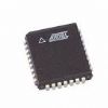
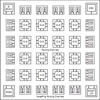
The xcs05-3vq100c is a FPGA. The xcs05-3vq100c is implemented with a regular, flexible, programmable architecture of Configurable Logic Blocks (CLBs), interconnected by a powerful hierarchy of versatile routing resources (routing channels), and surrounded by a perimeter of programmable Input/Output Blocks (IOBs), as seen in Figure 1. The xcs05-3vq100c has generous routing resources to accommodate the most complex interconnect patterns.
Parametrics
xcs05-3vq100c absolute maximum ratings: (1)VCC, Supply voltage relative to GND: –0.5 to +7.0 V; (2)VIN, Input voltage relative to GND(2,3): –0.5 to VCC +0.5 V; (3)VTS, Voltage applied to 3-state output(2,3): –0.5 to VCC +0.5 V; (4)TSTG, Storage temperature (ambient): –65 to +150 ℃; (5)TJ, Junction temperature Plastic packages: +125 ℃.
Features
xcs05-3vq100c features: (1)First ASIC replacement FPGA for high-volume production with on-chip RAM; (2)Density up to 1862 logic cells or 40,000 system gates; (3)Streamlined feature set based on XC4000 architecture; (4)System performance beyond 80 MHz; (5)Broad set of AllianceCORE and LogiCORE ; (6)predefined solutions available; (7)Unlimited reprogrammability; (8)Low cost; (9)Available in both 5V and 3.3V versions; (10)On-chip SelectRAM memory; (11)Fully PCI compliant; (12)Full readback capability for program verification and internal node observability; (13)Dedicated high-speed carry logic; (14)Internal 3-state bus capability; (15)Eight global low-skew clock or signal networks; (16)IEEE 1149.1-compatible Boundary Scan logic ; (17)Low cost plastic packages available in all densities; (18)Footprint compatibility in common packages; (19)Foundation Series: Integrated, shrink-wrap software; (20)Alliance Series: Dozens of PC and workstation third party development systems supported; (21)Fully automatic mapping, placement and routing; (22)3.3V supply for low power with 5V tolerant I/Os; (23)Power down input; (24)Higher performance; (25)Faster carry logic; (26)More flexible high-speed clock network; (27)Latch capability in Configurable Logic Blocks; (28)Input fast capture latch; (29)Optional mux or 2-input function generator on outputs; (30)12 mA or 24 mA output drive; (31)5V and 3.3V PCI compliant; (32)Enhanced Boundary Scan; (33)Express Mode configuration; (34)Chip scale packaging.
Diagrams
| Image | Part No | Mfg | Description |  |
Pricing (USD) |
Quantity | ||||||
|---|---|---|---|---|---|---|---|---|---|---|---|---|
 |
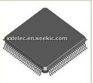
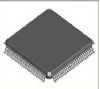
 XCS05-3VQ100C |
|
IC FPGA 5V C-TEMP 100-VQFP |
Data Sheet |
|
|
||||||
| Image | Part No | Mfg | Description | |
Pricing (USD) |
Quantity | ||||||
 |
XCS05 and XCS05XL |
Other |
|
Data Sheet |
Negotiable |
|
||||||
|
XCS05-3PC84C |
|
IC FPGA 5V C-TEMP 84-PLCC |
Data Sheet |
Negotiable |
|
||||||
|
XCS05-3VQ100C |
|
IC FPGA 5V C-TEMP 100-VQFP |
Data Sheet |
|
|
||||||
|
XCS05-3VQ100I |
|
IC FPGA 5V I-TEMP 100-VQFP |
Data Sheet |
Negotiable |
|
||||||
|
XCS05-4PC84C |
|
IC FPGA 5V C-TEMP 84-PLCC |
Data Sheet |
Negotiable |
|
||||||
|
XCS05-4VQ100C |
|
IC FPGA 5V C-TEMP 100-VQFP |
Data Sheet |
Negotiable |
|
||||||