(Hong Kong)

Product Summary
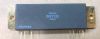
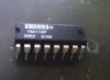
The ds92lv1210tmsa is a 16-40 MHz 10 bit bus LVDS serializer and deserializer. It transforms a 10-bit wide parallel CMOS/TTL data bus into a single high speed Bus LVDS serial data stream with embedded clock. The ds92lv1210tmsa receives the Bus LVDS serial data stream and transforms it back into a 10-bit wide parallel data bus and separates clock. The ds92lv1210tmsa may transmit data over heavily loaded backplanes or 10 meters of cable. The reduced cable, PCB trace count and connector size saves cost and makes PCB design layout easier. Clock-to-data and data-to-data skew are eliminated since one output will transmit both clock and all data bits serially. The powerdown pin is used to save power, by reducing supply current when either device is not in use. The Serializer has a synchronization mode that should be activated upon power-up of the device. The Deserializer will establish lock to this signal within 1024 cycles, and will flag Lock status. The embedded clock guarantees a transition on the bus every 12-bit cycle; eliminating transmission errors due to charged cable conditions. The ds92lv1210tmsa output pins may be TRI-STATE to achieve a high impedance state. The PLL can lock to frequencies between 16 MHz and 40 MHz.
Parametrics
ds92lv1210tmsa absolute maximum ratings: (1)Supply Voltage (VCC): -0.3V to +4V; (2)CMOS/TTL Input Voltage: -0.3V to (VCC +0.3V); (3)CMOS/TTL Output Voltage: -0.3V to (VCC +0.3V); (4)Bus LVDS Receiver Input Voltage: -0.3V to +3.9V; (5)Bus LVDS Driver Output Voltage: -0.3V to +3.9V; (6)Bus LVDS Output Short Circuit Duration: Continuous; (7)Junction Temperature: +150°C; (8)Storage Temperature: -65°C to +150°C; (9)Lead Temperature (Soldering, 4 seconds): +260°C.
Features
ds92lv1210tmsa features: (1)Guaranteed transition every data transfer cycle; (2)Single differential pair eliminates multi-channel skew; (3)Flow-through pinout for easy PCB layout; (4)400 Mbps serial Bus LVDS bandwidth (at 40 MHz clock); (5)10-bit parallel interface for 1 byte data plus 2 control bits; (6)Synchronization mode and LOCK indicator; (7)Programmable edge trigger on clock; (8)High impedance on receiver inputs when power is off; (9)Bus LVDS serial output rated for 27Ω load; (10)Small 28-lead SSOP package-MSA.
Diagrams

| Image | Part No | Mfg | Description |  |
Pricing (USD) |
Quantity | ||||
|---|---|---|---|---|---|---|---|---|---|---|
 |
 DS92LV1210TMSA/NOPB |
|
IC DESERIALIZER 10-BIT 28-SSOP |
Data Sheet |
Negotiable |
|
||||
|
DS92LV1210TMSAX |
|
IC DESERIALIZER 10BIT 28-SSOP |
Data Sheet |
Negotiable |
|
||||