(Hong Kong)

Product Summary
The w45nm50 is a new revolutionary mosfet technology that associates the Multiple Drain pro-cess with the Company’s PowerMESH horizontal layout. The w45nm50 has an outstanding low on-resistance, impressively high dv/dt and excellent avalanche characteristics. The adoption of the Company’s proprietary strip technique yields overall dynamic performance that is significantly better than that of similar competition’s products.The application of the w45nm50 includes the mdmesh family is very suitable for increasing power density of high voltage converters allowing system miniaturization and higher efficiencies.
Parametrics
w45nm50 absolute maximum ratings: (1)Gate- source Voltage: ±30 V; (2)Drain Current (continuous) at TC = 25℃: 45 A; (3)Drain Current (continuous) at TC = 100℃: 28.4 A; (4)Drain Current (pulsed): 180 A; (5)Total Dissipation at TC = 25℃: 417 W; (6)Derating Factor: 2.08 W/℃; (7)Peak Diode Recovery voltage slope: 15 V/ns; (8)Storage Temperature: –65 to 150 ℃; (9)Max. Operating Junction Temperature: 150 ℃.
Features
w45nm50 features: (1)typical rds(on) = 0.08; (2)high dv/dt and avalanche capabilities; (3)100% avalanche tested; (4)low input capacitance and gate charge; (5)low gate input resistance; (6)tight process control and high; (7)manufacturing yields.
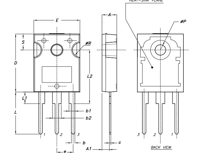
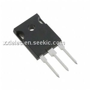
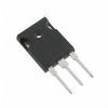
Diagrams