(Hong Kong)

Product Summary
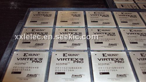
The XC2VP40 is an FPGA for designs that are based on IP cores and customized modules. The family incorporates multi-gigabit transceivers and PowerPC CPU blocks in Virtex-II Pro Series FPGA architecture. The XC2VP40 empowers complete solutionsfor telecommunication, wireless, networking, video, and DSP applications. The leading-edge 0.13 μm CMOS nine-layer copper process and Virtex-II Pro architecture are optimized for high performance designs in a wide range of densities. Combining a wide variety of flexible features and IP cores, the XC2VP40 enhances programmable logic design capabilities and is a powerful alternative to mask-programmed gate arrays.
Parametrics
XC2VP40 absolute maximum ratings: (1)VCCINT, Internal supply voltage relative to GND: –0.5 to 1.6 V; (2)VCCAUX, Auxiliary supply voltage relative to GND: –0.5 to 3.0 V; (3)VCCO, Output drivers supply voltage relative to GND: –0.5 to 3.75 V; (4)VBATT, Key memory battery backup supply: –0.5 to 4.05 V; (5)VREF, Input reference voltage: –0.3 to 3.75 V; (6)VIN: 3.3V I/O input voltage relative to GND (user and dedicated I/Os) –0.3 to 4.05 V; 2.5V or below I/O input voltage relative to GND (user and dedicated I/Os): –0.5 to VCCO + 0.5 V; (7)VTS: Voltage applied to 3-state 3.3V output (user and dedicated I/Os): –0.3 to 4.05 V; Voltage applied to 3-state 2.5V or below output (user and dedicated I/Os): –0.5 to VCCO + 0.5 V; (8)TSTG, Storage temperature (ambient): -65 to +150℃; (9)TJ, Maximum junction temperature: +125℃.
Features
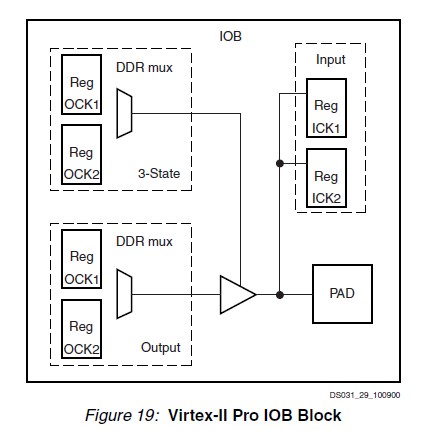
XC2VP40 features: (1)High-Performance Platform FPGA Solution, Including: Up to twenty RocketIO or RocketIO X embedded Multi-Gigabit Transceivers (MGTs); Up to two IBM PowerPC RISC processor blocks; (2)Based on Virtex-II?Platform FPGA Technology: Flexible logic resources; SRAM-based in-system configuration; Active Interconnect technology; SelectRAM memory hierarchy; Dedicated 18-bit x 18-bit multiplier blocks; High-performance clock management circuitry; SelectI/O Ultra technology; XCITE Digitally Controlled Impedance (DCI) I/O.
Diagrams
| Image | Part No | Mfg | Description |  |
Pricing (USD) |
Quantity | ||||||
|---|---|---|---|---|---|---|---|---|---|---|---|---|
 |
 XC2VP40-5FF1148I |
|
IC FPGA VIRTEX-II PRO 1148FFBGA |
Data Sheet |
|
|
||||||
|
XC2VP40-5FF1152C |
Other |
|
Data Sheet |
Negotiable |
|
||||||
|
XC2VP40-5FF1152I |
|
IC FPGA VIRTEX-II PRO 1152FFBGA |
Data Sheet |
|
|
||||||
|
XC2VP40-5FFG1148C |
|
IC FPGA VIRTEX-II PRO 1148-FBGA |
Data Sheet |
|
|
||||||
|
XC2VP40-5FFG1148I |
|
IC FPGA VIRTEX-II PRO 1148-FBGA |
Data Sheet |
|
|
||||||
|
XC2VP40-5FFG1152C |
|
IC VIRTEXIIPRO FPGA 40K 1152FBGA |
Data Sheet |
|
|
||||||
|
XC2VP40-6FFG1148C |
|
IC FPGA VIRTEX-II PRO 1148-FBGA |
Data Sheet |
|
|
||||||
 |
XC2VP40-5FGG676C |
|
IC VIRTEXIIPRO FPGA 40K 676BGA |
Data Sheet |
|
|
||||||