(Hong Kong)

Product Summary
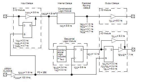
The a1240apg132m is an ACT 2 Family FPGA. The a1240apg132m presents a two-module architecture, consisting of C-modules and S-modules. The a1240apg132m is optimized for both combinatorial and sequential designs. Based on Actel’s patented channeled array architecture, the a1240apg132m provides significant enhancements to gate density and performance while maintaining downward compatibility with the ACT 1 design environment and upward compatibility with the ACT 3 design environment. The a1240apg132m is implemented in silicon gate, 1.0-μm, two-level metal CMOS, and employ Actel’s PLICE antifuse technology.
Parametrics
a1240apg132m absolute maximum ratings: (1)VCC, DC supply voltage: –0.5 to +7.0 V; (2)VI, Input voltage: –0.5 to VCC + 0.5 V; (3)VO, Output voltage: –0.5 to VCC + 0.5 V; (4)IIO, I/O source sink current: ±20 mA; (5)TSTG, Storage temperature: –65 to +150 ℃.
Features
a1240apg132m features: (1)Up to 8,000 Gate Array Gates; (2)Replaces up to 200 TTL Packages; (3)Replaces up to eighty 20-Pin PAL Packages; (4)Design Library with over 500 Macro Functions; (5)Single-Module Sequence Functions; (6)Wide-Input Combinatorial Functions; (7)Up to 1,232 Programmable Logic Modules; (8)Up to 998 Flip-Flops; (9)Datapath Performance at 105 MHz; (10)16-Bit Accumulator Performance to 39 MHz; (11)Two In-Circuit Diagnostic Probe Pins Support Speed Analysis to 50 MHz; (12)Two High-Speed, Low-Skew Clock Networks; (13)I/O Drive to 10 mA; (14)Nonvolatile, User Programmable; (15)Logic Fully Tested Prior to Shipment; (16)1.0 micron CMOS Technology.
Diagrams